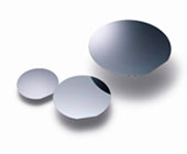
Gallium Nitride HEMT Epiwafer
Gallium nitride (GaN) is used as the wide band gap material for next generation power semiconductors and high frequency devices. We achieved high voltage resistance and good flatness on the Gallium Nitride HEMT Epiwafers using our proprietary buffer layers. (GaN on Si HEMT Epiwafers)
We are also engaged in the development of p-GaN cap layers and AlGaN DH structure for the realization of normally-off HEMT Epiwafers.
We also handle GaN Epiwafers on silicon carbide (SiC) and sapphire and AIN templates for high-quality LED (on sapphire wafer).
Applications (GaN on Si HEMT Epiwafer)
- For power semiconductors: Inverter and AC-DC converter
- For high-frequency devices: For mobile phone base stations
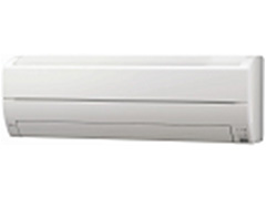
Inverter for air conditioner etc.
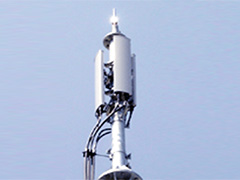
For high frequency devices such as mobile phone base stations
Product features(GaN on Si HEMT Epiwafer)
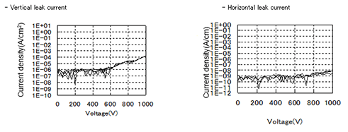
- High voltage resistance (1000V) and low leak current (1E-6A)
- Crack-free
- Good bow feature (Bow < 50μm)
- Wafer size (3, 4, and 6 inches)
- Capable of handling thick films (4.8μm)
- p-GaN cap layer and alGaN DH structure
Product characteristics (GaN on Si HEMT Epiwafer)
- Standard HEMT Structure
| Layer | Composition | Thickness | x |
| 4 | GaN | 1nm | |
| 3 | AlxGa1-xN | 30nm | 0.25 |
| 2 | GaN | 1500nm | |
| 1 | Buffer | 3300nm | |
| Substrate | Si | 625um |
- Substrate
| Material | Silicon |
| Orientation | <111> |
| Crystal growth method | CZ |
| Type | p type |
| Size(inch) | 3,4,6 |
| Thickness(um) | 625 or 675 |
| Backside | rough |
- Electrical properties
| Hall measurement | Typical value |
| Sheet resistance(ohm/sq) | 400 |
| Carrier density(/cm2) | 1.00E+13 |
| Mobility(cm2/Vs) | 1550 |
- Vertical/Horizontal leak current
- Notes
- - Recommended use: Power switching device
- - The values and characteristics shown here are typical values.
- - We will adjust the structure and characteristics on request.
- - We can meet your requests for the p-GaN cap layer and AlGaN buffer structure.
Product characteristics (AIN template)
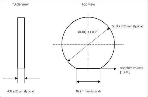
| Substrate: | c-plane sapphire |
| Crystal Structure of AlN Epitaxial Layer: | wurtzite |
| Diameter: | 50.8 mm ± 0.25 mm (typical) |
| Thickness of Substrate: | 430 μm ± 25 μm (typical) |
| Thickness of AlN Epitaxial Layer: | 1 μm ± 0.3 μm (typical) |
| Surface: | c-plane AlN, as grown effective area < 40 mmΦ (typical) no cracks by a visual inspection. |
| Backside: | rough |
| FWHM of X-ray ω-scan rocking curve: | < 150 arcsec for (0002) (typical) |
| Conductivity: | insulating |
| Packing: | packaged fluoroware container and vacuum-packed. |
For inquiries regarding the contents of this page, please contact...
DOWA ELECTRONICS MATERIALS CO., LTD. Semiconductor Business Unit22F, Akihabara UDX, 4-14-1, Sotokanda, Chiyoda-ku, Tokyo, 101-0021 Japan
TEL : +81-3-6847-1253 FAX : +81-3-6847-1260