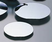
Gallium Arsenide Wafer
Our Gallium Arsenide Wafers are used in a wide range of fields including electronics devices such as laser applications for DVD, LED, and mobile phones.
Applications
- The wafers are used in high-output LDs, VCSEL, micro LEDs and display LEDs.
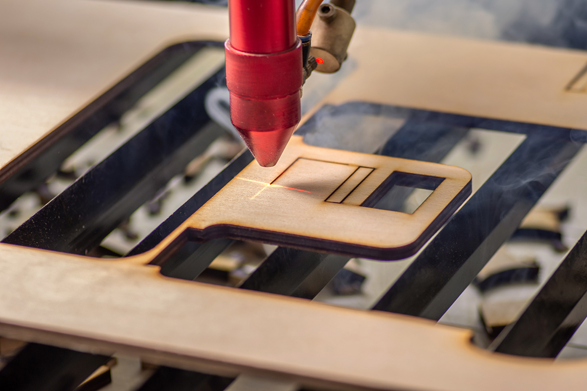
High-output industrial laser
Product features
- VGF and LEC methods are used to develop single crystals.
- The wafers are characterized by highly controlled carrier density and low EPD.
Product characteristics
VGF-n type
| VGF-n type, LD grade | VGF-n type, LED grade | |||||||
| Crystal growth method | VGF (vertical gradient freezing) method | VGF (vertical gradient freezing) method | ||||||
| Dopant and conductive type | N type: Si-doped | N type: Si-doped | ||||||
| Carrier density | N-type (0.4-4)×1018 cm-3 (Adjustable within the above range) |
N-type (0.4-4)×1018 cm-3 (Adjustable within the above range) |
||||||
| Dislocation density(EPD) (cm-2) |
EPDave</=500(LED) EPDmax</=5000(LED) |
EPDave</=500(LED) EPDmax</=5000(LED) |
||||||
| Size | 6-inch | 4-inch | 3-inch | 2-inch | 6-inch | 4-inch | 3-inch | 2-inch |
| Plane orientation |
1. (100)±0.1° 2. (100) off α°±0.1° towards (011) or (01-1) etc. 3. We will aim to meet your requests. |
1. (100)±0.1° 2. (100) off α°±0.1° towards (011) or (01-1) etc. 3. We will aim to meet your requests. |
||||||
| Diameter (mm) |
150.0±0.1 | 100.0±0.1 | 76.0±0.1 76.2±0.1 |
50.0±0.1 50.8±0.1 |
150.0±0.2 | 100.0±0.2 | 76.0±0.2 76.2±0.2 |
50.0±0.2 50.8±0.2 |
| Thickness (μm) |
450-675 ±15 |
350-625 ±15 |
300-600 ±15 |
240-450 ±15 |
450-675 ±20 |
350-625 ±20 |
300-600 ±20 |
240-450 ±20 |
|
Orientation flat length OF(mm) IF(mm) |
48.0±1.0 30.0±1.0 |
32.5±1.0 18.0±1.0 |
22.0±1.0 12.0±1.0 |
16.0±1.0 8.0±1.0 |
48.0±1.0 30.0±1.0 |
32.0±1.0 18.0±1.0 |
22.0±1.0 12.0±1.0 |
16.0±1.0 8.0±1.0 |
| (Adjustable upon request) | (Adjustable upon request) | |||||||
|
Orientation flat direction OF(mm) IF(mm) |
EJ (Dove-Tail):[OF] (0-1-1)±0.05°/ [IF](0-11)±0.5° or SEMI US (V-Groove):[OF] (01-1)±0.05°/ [IF](011)±0.5° (Adaptable to both cleavage and bevel) |
EJ (Dove-Tail):[OF] (0-1-1)±0.5°/ [IF](0-11)±0.5° or SEMI US (V-Groove):[OF] (01-1)±0.5°/ [IF](011)±0.5° |
||||||
| Notch | OK | Not allowed | Not allowed | Not allowed | OK | Not allowed | Not allowed | Not allowed |
| Edge rounding | Beveled | Beveled | ||||||
| Metalworking precision TTV(μm) |
<5.0 | <5.0 | <5.0 | <5.0 | <10.0 | <10.0 | <10.0 | <10.0 |
| Metalworking precision Warp(μm) |
<10.0 | <10.0 | <10.0 | <10.0 | <15.0 | <15.0 | <15.0 | <15.0 |
| Surfacing Surface |
Mirror | Mirror | ||||||
| Surfacing Back |
Post-lap etching (mirror processing is also available) | Post-lap etching (mirror processing is also available) | ||||||
| Surface processing | Epi-ready | Epi-ready | ||||||
| Laser mark | Option | Option | ||||||
| Packaging form | Cassette | Cassette or individual packaging tray | Cassette | Cassette or individual packaging tray | ||||
VGF-p type
| VGF-p type Zn-doped | VGF-p type Zn- and Si-doped | ||||
| Carrier density | VGF (vertical gradient freezing) method | VGF (vertical gradient freezing) method | |||
| Dopant and conductive type | P type: Zn-doped | P type: Zn- and Si-doped | |||
| Carrier density | P-type (0.5-3)×1019 cm-3 (Adjustable within the above range) |
P-type (0.5-3)×1019 cm-3 (Adjustable within the above range) |
|||
| Dislocation density (EPD) | (cm-2) |
EPDave</=3000 EPDmax</=10000 |
EPDave</=1500 EPDmax</=10000 |
||
| Size | 3-inch | 2-inch | 3-inch | 2-inch | |
| Plane orientation | 1. (100)±0.1° 2. (100) off α°±0.1° towards (011) or (01-1) etc. 3. We will aim to meet your requests. |
1. (100)±0.1° 2. (100) off α°±0.1° towards (011) or (01-1) etc. 3. We will aim to meet your requests. |
|||
| Diameter | (mm) | 76.0±0.1 76.2±0.1 |
50.0±0.1 50.8±0.1 |
76.0±0.1 76.2±0.1 |
50.0±0.1 50.8±0.1 |
| Thickness | (μm) | 300-600 ±15 |
240-450 ±15 |
300-600 ±15 |
240-450 ±15 |
| Orientation flat length |
OF(mm) IF(mm) |
22.0±1.0 12.0±1.0 |
16.0±1.0 8.0±1.0 |
22.0±1.0 12.0±1.0 |
16.0±1.0 8.0±1.0 |
| (Adjustable upon request) | (Adjustable upon request) | ||||
| Orientation flat direction |
OF(mm) IF(mm) |
EJ (Dove-Tail):[OF] (0-1-1)±0.05°/ [IF](0-11)±0.5° or SEMI US (V-Groove):[OF] (01-1)±0.05°/ [IF](011)±0.5° (Adaptable to both cleavage and bevel) |
EJ (Dove-Tail):[OF] (0-1-1)±0.05°/ [IF](0-11)±0.5° or SEMI US (V-Groove):[OF] (01-1)±0.05°/ [IF](011)±0.5° (Adaptable to both cleavage and bevel) |
||
| Edge rounding | Beveled | Beveled | |||
| Metalworking precision | TTV(μm) | <5.0 | <5.0 | <5.0 | <5.0 |
| Warp(μm) | <10.0 | <10.0 | <10.0 | <10.0 | |
| Surfacing | Surface | Mirror | Mirror | ||
| Back | Post-lap etching (mirror processing is also available) | Post-lap etching (mirror processing is also available) | |||
| Surface processing | Epi-ready | ||||
| Laser mark | Option | Option | |||
| Packaging form | Cassette or individual packaging tray | Cassette or individual packaging tray | |||
Semi-insulating properties
| VGF semi-insulating properties | LEC semi-insulating properties | |||||
| Carrier density | VGF (vertical gradient freezing) method | LEC (Liquid Encapsulated Czochralski) method | ||||
| Dopant and conductive type | Semi-insulating properties: Undoped (C-doped) | Semi-insulating properties: Undoped (C-doped) | ||||
| Resistivity (at 25℃) |
>/=1×107 Ω cm (Adjustable within the above range) |
>/=1×107 Ω cm (Adjustable within the above range) |
||||
| Dislocation density (EPD) (cm-2) |
EPDave</=5000 | EPDave</=10^5 | ||||
| Size | 4-inch | 3-inch | 2-inch | 4-inch | 3-inch | 2-inch |
| Plane orientation |
1. (100)±0.1° 2. (100) off 2°±0.1° towards (110) etc. 3. We will aim to meet your requests.。 |
1. (100)±0.1° 2. (100) off 2°±0.1° towards (110) etc. 3. We will aim to meet your requests.。 |
||||
| Diameter (mm) |
100.0±0.1 |
76.0±0.1 76.2±0.1 |
50.0±0.1 50.8±0.1 |
100.0±0.1 |
76.0±0.1 76.2±0.1 |
50.0±0.1 50.8±0.1 |
| Thickness (μm) |
450-625 ±15 |
350-625 ±15 |
300-450 ±15 |
450-625 ±15 |
350-625 ±15 |
300-450 ±15 |
|
Orientation flat length OF(mm) IF(mm) |
32.0±1.0 18.0±1.0 |
22.0±1.0 12.0±1.0 |
16.0±1.0 8.0±1.0 |
32.0±1.0 18.0±1.0 |
22.0±1.0 12.0±1.0 |
16.0±1.0 8.0±1.0 |
| (Adjustable upon request) | (Adjustable upon request) | |||||
|
Orientation flat direction OF(mm) IF(mm) |
EJ (Dove-Tail):[OF] (0-1-1)±0.5°/ [IF](0-11)±0.5° or SEMI US (V-Groove):[OF] (01-1)±0.5°/ [IF](011)±0.5° |
EJ (Dove-Tail):[OF] (0-1-1)±0.5°/ [IF](0-11)±0.5° or SEMI US (V-Groove):[OF] (01-1)±0.5°/ [IF](011)±0.5° |
||||
| Edge rounding | Beveled | Beveled | ||||
| Metalworking precision TTV(μm) |
<5.0 | <5.0 | <5.0 | <5.0 | <5.0 | <5.0 |
| Metalworking precision TIR(μm) |
<5.0 | <5.0 | <5.0 | <5.0 | <5.0 | <5.0 |
| Metalworking precision Warp(μm) |
<10.0 | <10.0 | <10.0 | <10.0 | <10.0 | <10.0 |
| Surfacing Surface |
Post-lap etching (mirror processing is also available) | Post-lap etching (mirror processing is also available) | ||||
| Surfacing Back |
Post-lap etching (mirror processing is also available) | Post-lap etching (mirror processing is also available) | ||||
| Surface processing | Epi-ready | Epi-ready | ||||
| Laser mark | Option | Option | ||||
| Packaging form | Cassette or individual packaging tray | Cassette or individual packaging tray | ||||
For inquiries regarding the contents of this page, please contact...
DOWA ELECTRONICS MATERIALS CO., LTD. Semiconductor Business Unit22F, Akihabara UDX, 4-14-1, Sotokanda, Chiyoda-ku, Tokyo, 101-0021 Japan
TEL : +81-3-6847-1253 FAX : +81-3-6847-1260