


Standard HEMT Structure
| Layer | Composition | Thickness | x |
| 4 | GaN | 1nm | |
| 3 | AlxGa1-xN | 30nm | 0.25 |
| 2 | GaN | 1500nm | |
| 1 | Buffer | 3300nm | |
| Substrate | Si | 625um |
Substrate
| Material | Silicon |
| Orientation | <111> |
| Crystal growth method | CZ |
| Type | p type |
| Size(inch) | 3,4,6 |
| Thickness(um) | 625 or 675 |
| Backside | rough |
Electrical properties
| Hall measurement | Typical value |
| Sheet resistance(ohm/sq) | 400 |
| Carrier density(/cm2) | 1.00E+13 |
| Mobility(cm2/Vs) | 1550 |
Vertical/Horizontal leak current

- Remarks
Recommended application: Switching Devices
Please note that structure, substrate and electrical properties are typical value.
Customizations are available on request.
p-GaN cap layer and AlGaN DH structure are available.
Recommended application: Switching Devices
Please note that structure, substrate and electrical properties are typical value.
Customizations are available on request.
p-GaN cap layer and AlGaN DH structure are available.
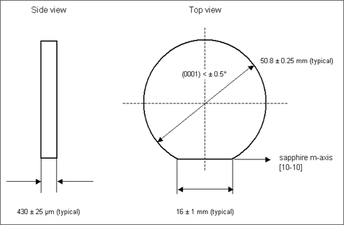
| Substrate: | c-plane sapphire |
| Crystal Structure of AlN Epitaxial Layer: | wurtzite |
| Diameter: | 50.8 mm ± 0.25 mm (typical) |
| Thickness of Substrate: | 430 μm ± 25 μm (typical) |
| Thickness of AlN Epitaxial Layer: | 1 μm ± 0.3 μm (typical) |
| Surface : | c-plane AlN, as grown effective area < 40 mmΦ (typical) no cracks by a visual inspection. |
| Backside : | rough |
| FWHM of X-ray ω-scan rocking curve : | < 150 arcsec for (0002) (typical) |
| Conductivity : | insulating |
| Packing : | packaged fluoroware container and vacuum-packed. |
| e-mail to: hemt@dowa.co.jp |